
Machine learning with python

Instructor
Skill Bridge Interns
Reviews
Course Overview
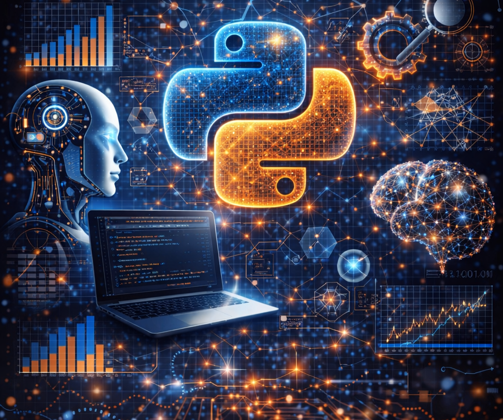
Machine Learning with Python:
The Machine Learning with Python internship program is designed to provide a strong foundation in building intelligent systems using data-driven techniques. This program focuses on practical implementation of machine learning algorithms using Python and its powerful libraries.
During the internship, participants gain hands-on experience with tools like NumPy, Pandas, Matplotlib, Scikit-learn, and TensorFlow, enabling them to work with real-world datasets and develop predictive models.
Interns will:
- Understand core concepts of machine learning algorithms (supervised & unsupervised learning)
- Perform data preprocessing, feature selection, and model evaluation
- Build models like linear regression, logistic regression, decision trees, and clustering
- Work on real-world projects such as prediction systems and classification tasks
- Visualize data and results using Matplotlib and Seaborn
- Learn basics of model optimization and performance tuning